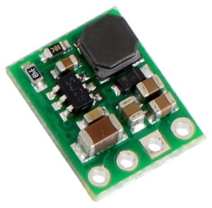
We've discovered that the linear voltage regulators included in the chipKIT Max32 are very inefficient when providing with more than 9v of input voltage, and when a vehicle provides nearly 13V+ they can get so hot that it effects normal operation. If you intend to leave the chipKIT plugged into the vehicle for more than a few hours, we strongly recommend this alternative power supply.
Thanks to Basavaraj Tonshal and James Rankin II for their engineering work and for writing this report, and to Zac Nelson for additional engineering - all from Ford.
The chipKIT Max32 uses two linear voltage regulators, the NCP1117 and MCP1725. The NCP1117 is the main regulator that steps down the input voltage to 5V. This is used as input to the MCP1725, which steps the 5V down to 3.3V for the PIC32.
The NCP1117 is a linear voltage regulator, with a transistor acting like a dynamic resistor (reference pdf). The resistance varies as the load increases to produce constant DC output. The power dissipation is directly proportional to the junction temperature of the transistor.
The power dissipation P is given by
P = (VIN - VOUT) * IL
The average load from the chipKIT Max32 with the Network Shield and an RN-42 Bluetooth module is about 250mA. When the chipKIT is powered by the OBD-II pins, with ~13.5V available on OBD-II pin, it needs to be stepped down to 5V. The power dissipated is about:
P = (13.5 - 5) * 250 / 1000 = 2.125 Watts
The copper area available for SOT-223 package that is being used with NCP1117 is too small to dissipate the heat generated. So basically we are generating a lot of heat and there is no place for the heat to dissipate. The issue is greater when the ambient temperature is high and the hardware is enclosed in a box. When the voltage regulator temperature increases the internal thermal protection triggers thermal shutdown of the voltage regulator and thus the VI hardware starts behaving erratically.
There are various solutions to address this issue:
Providing heat sink is not an effective solution and also the space available is limited to fit in a heat sink. One can also think of putting an extra voltage regulator that will step down the OBD-II pin voltage from ~13.5V to 8V and then feed the output from the 8V voltage regulator to on board NCP1117.
We suggest bypassing the existing voltage regulator with a switching type regulator. Switching regulators work using high frequency switching in combination with energy storage elements inductor and capacitor to produce a constant stepped down DC output. There are no dissipative elements in the circuit. The advantages of switching type regulators are higher efficiency, less heat and smaller size.
This table shows normal and sleep mode current draws with different voltage regulators running VI firmware. The test is done with a DC power supply at 14.2V with box open, using the built-in regulators and the Pololu 5V, 600mA Step-Down Voltage Regulator D24V6F5.
| Regulators | Normal Current Draw (mA) | Sleep Current Draw (mA) |
|---|---|---|
| Built-in linear | 172 | 45 |
| Switching regulator | 72 | 20 |
Finally, here's how the external switching voltage regulators can be connected to chipKIT Max32 and Network shield. When bypassing the onboard voltage regulator the POWER SELECT jumper JP1 must be set to JP1 (reference PDF).

